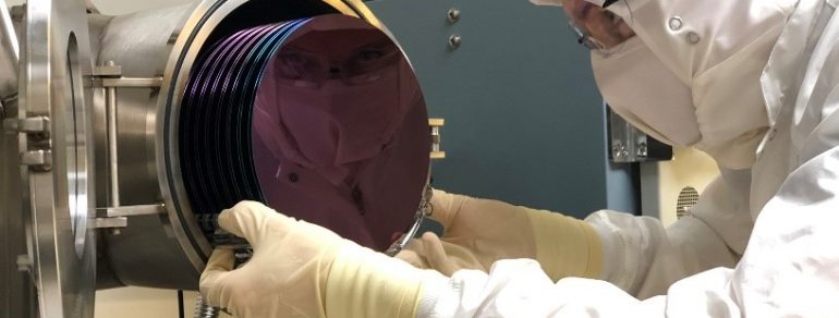
Outlining CVD of Graphene for Wafers

Since graphene flakes were first isolated via adhesive exfoliation in 2004, the material has arisen in several new permutations. Powders, ribbons, and graphene wafers have all been generated using novel techniques such as epitaxial growth in specialist reaction chambers. These techniques have rapidly eclipsed exfoliation in the race to commercialize graphene manufacturing due to the inherent difficulties of producing large area graphene sheets using adhesive tape isolation.
Isolating graphene through exfoliation requires multiple sequences of adhesive cleaving with high-strength tape. This yields small scale flakes of monolayer graphene with millimeter proportions, which are then deposited onto a functional substrate. It is an extremely difficult process to scale, which explains why manufacturers are increasingly turning towards methods like chemical vapor deposition (CVD) to produce large area graphene for transfer on to wafers and other substrates.
In this blog post, Grolltex explores the CVD generation of graphene for wafers in more detail.
What is Monolayer Graphene for Wafers?
Graphene monolayer sheets comprised of carbon (C) atoms are covalently bound in continuous hexagonal lattices. While graphene flakes are limited to a few millimeters, large area graphene sheets or films for transfer on to wafers are typically between 4—8” in diameter. These graphene wafers are increasingly sought after for direct integration into commercial production lines given their outstanding mechanical and especially their electronic and sensing properties.
Explaining CVD of Graphene for Wafers
CVD is a method of generating graphene in a specialist reaction chamber. This is performed by condensing reactant gases on a suitable substrate material in an ultra-high vacuum (UHV). Although the nature of the interaction between carbon atoms and the growth substrate has proven difficult to characterize, research has determined that the bonding affinity between carbon molecules and the growth substrate is a vital metric for achieving the electronic band structure of monolayer graphene.
Electronic substrates used to support monolayer graphene are often described as slices as they can be extracted from larger crystal macrostructures via wire-sawing. This is an extremely precise process that succeeds synthetic crystal growth at high temperatures and precedes several additional stages of substrate finishing. Manufacturers aim to achieve outstanding degrees of lateral planarization prior to CVD to facilitate graphene growth. It is now possible to routinely generate graphene on a range of material substrates including silicon carbide (SiC), platinum (Pt), and cobalt (Co) slices as well as copper (Cu) foils. CVD graphene as produced on optimized copper substrates, however, is known to produce some of the highest quality, largest grain single-layer graphene available.
Graphene from Grolltex
At Grolltex, our core competency is in the manufacture of exceptionally high-quality large area, single layer graphene that can be transferred to substrates of the customers choosing. We can also synthesize and transfer single layer hexagonal boron nitride (hBN) for use on the customer’s substrate or for layering to create heterostructures with graphene in any layer combination desired in up to 8” (200mm) diameter sizes.
If you would like to learn more about the challenges of generating graphene for wafers by CVD, read our previous blog post: Exploring the History of Graphene Production. Otherwise, contact us directly with any questions.
