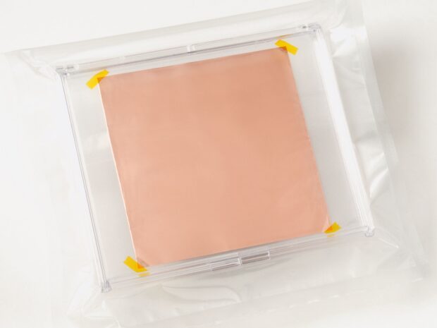
GRA-CU-6
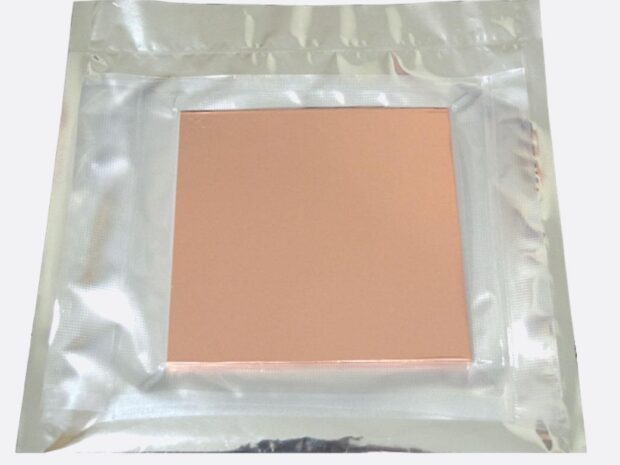
Monolayer graphene film on copper foil, 6" × 6"
CVD monolayer graphene film on copper foil. Single-atom-thick conductor for transfer onto your substrate, sensors, electrodes and heterostructures. In stock.

CVD monolayer materials · Made in San Diego, USA
Monolayer films up to 8 inches, grown by chemical vapor deposition and transferred to the substrate you build on. Stock sizes ship from the shelf; every unit carries a specification sheet measured from its own batch.
In stock, priced, and shipping 1–3 days from payment. Free shipping within the US.
GRA-CU-6
CVD monolayer graphene film on copper foil. Single-atom-thick conductor for transfer onto your substrate, sensors, electrodes and heterostructures. In stock.
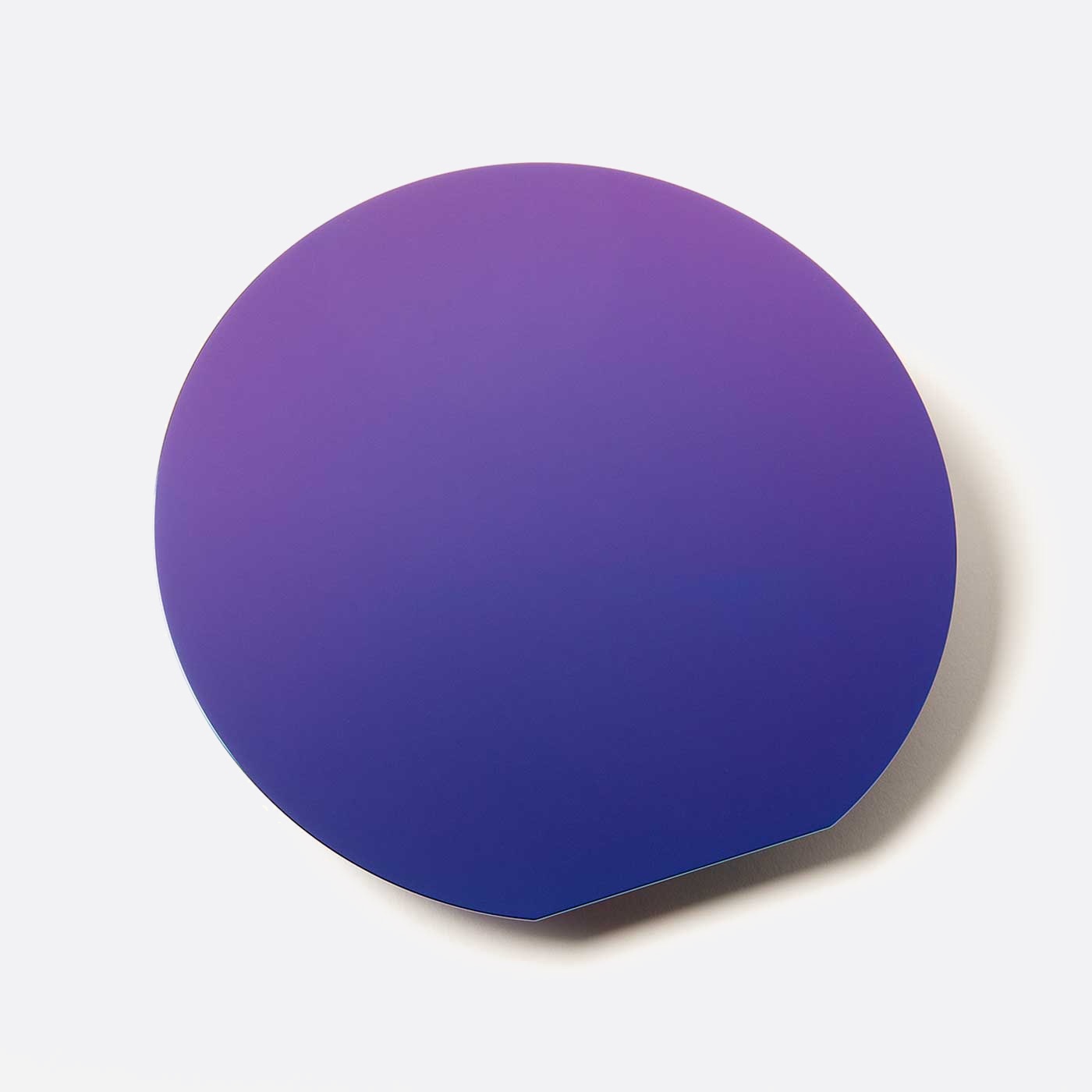
HBN-CU-6
CVD monolayer hexagonal boron nitride (hBN) film on copper foil. Insulating 2D complement to graphene for dielectrics, encapsulation and heterostructures. Coming soon.
Relocation and process requalification · 2026
A new cleanroom. An updated production line. New quality protocols. Every batch ships with its own data set.
A new San Diego facility built around the growth and transfer line rather than inherited from it. Class 100 cleanroom, laid out so the material never leaves controlled air between growth and pack-out.
Production equipment updated and requalified end to end, from growth through transfer to final inspection. Ultra-fast cooldowns give cleaner films, with lower defect density and lower adlayer counts.
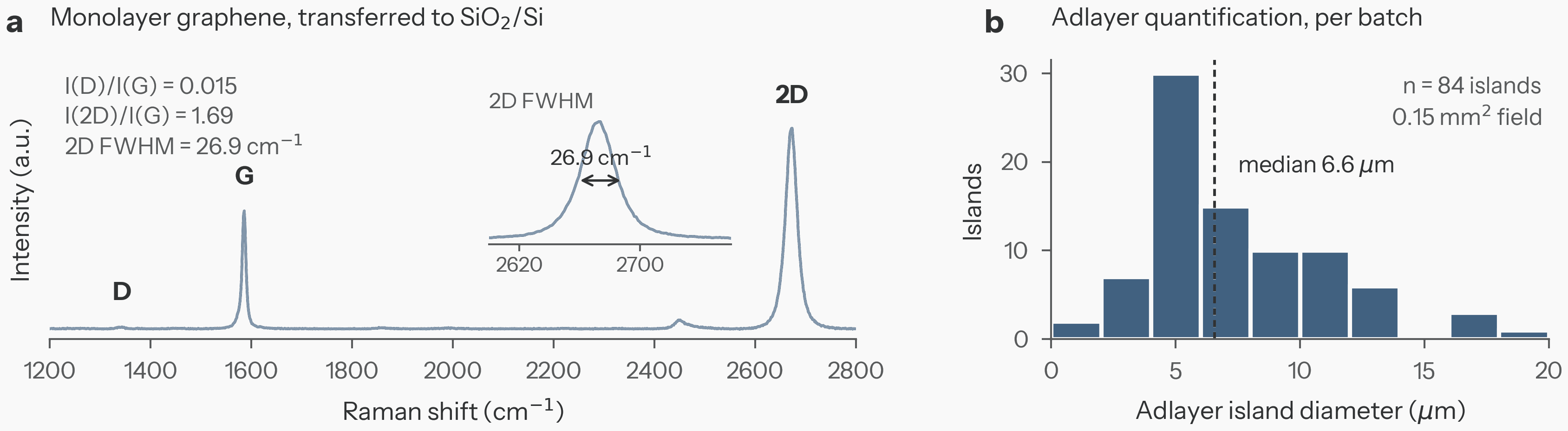
New and updated QC protocols, applied to every batch rather than sampled across a lot. Daily static-vacuum monitoring. Raman calibrated against a standard.
Oxygen-free copper foil rolled for Grolltex by a German mill to our own specification: OFE-Cu58 / ASTM C101, ultra-smooth, with a mirror surface finish and consistent character roll to roll.
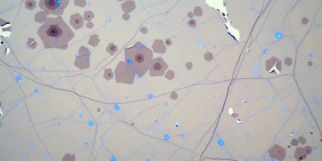
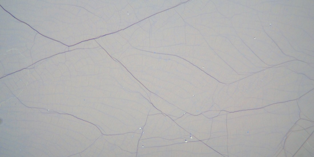
>97% T, 100% coverage
D/G, 2D FWHM, peak table
count, size, area fraction
density and orientation
serialised, txt + csv
Sizes, substrates and stacks quoted per configuration.
GRA-XFER
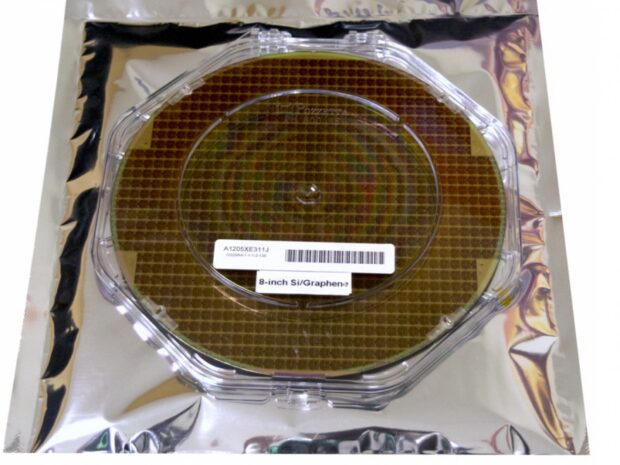
Monolayer graphene transferred onto Si/SiO₂, quartz, or the wafer you send us, up to 8 inches.
HBN-XFER
Monolayer hBN transferred onto your device substrate as a gate dielectric or encapsulation layer.
GRA-HBN
A layer of hBN beneath graphene. The close lattice match raises electron mobility for sensing and transistors.
Supplying researchers worldwide since 2017 — top universities, Fortune 500 companies and national laboratories.
More than 250 citations on Google Scholar report work using Grolltex materials.
Grown, transferred and packaged in San Diego, California — not resold from an overseas supplier.
Optical coverage, a Raman peak table, adlayer and wrinkle statistics — measured on your batch, not a representative lot.
Send us your wafer and we transfer graphene, hBN, or a stack of both onto it, up to 8 inches.
Stock sizes are listed and buyable online, with purchase orders accepted from institutions.
Send your wafer and we transfer monolayer graphene, hBN, or a graphene-on-hBN heterostructure onto it.