HBN-XFER
hBN transferred to your substrate
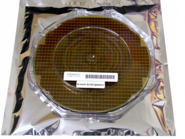
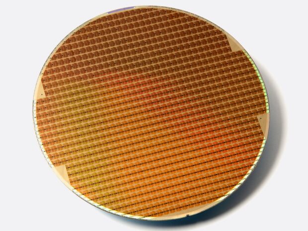
Monolayer hBN transferred onto your device substrate as a gate dielectric or encapsulation layer.
Request pricing
Details — hBN transferred to your substrate

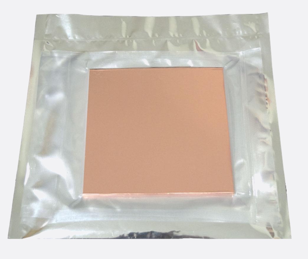
$890.00
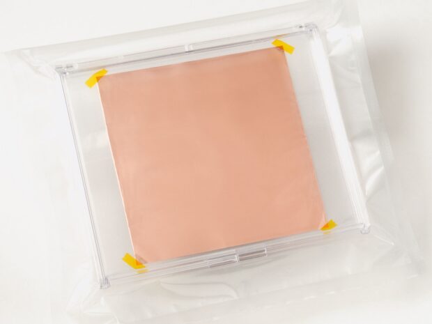
CVD monolayer hexagonal boron nitride (hBN) film on copper foil. Insulating 2D complement to graphene for dielectrics, encapsulation and heterostructures. In stock.
Ships from San Diego 1–3 days from payment. Purchase orders accepted from institutions.
| Specification | Value |
|---|---|
| Material | Monolayer hexagonal boron nitride |
| Layers | 1 |
| Sheet size | 6" × 6" |
| Substrate | Oxygen-free copper foil, 25 μm |
| Copper spec | OFE-Cu58 / ASTM C101 |
| Surface finish | Ultra-smooth, mirror |
| Coverage | ≥95% guaranteed, typically 100% |
| Band gap | ~5.9 eV |
| Fabrication | Class 100 cleanroom |
| Packaging | Double vacuum wrapped, N₂ |
Representative data. The unit you receive ships with measurements from its own batch.

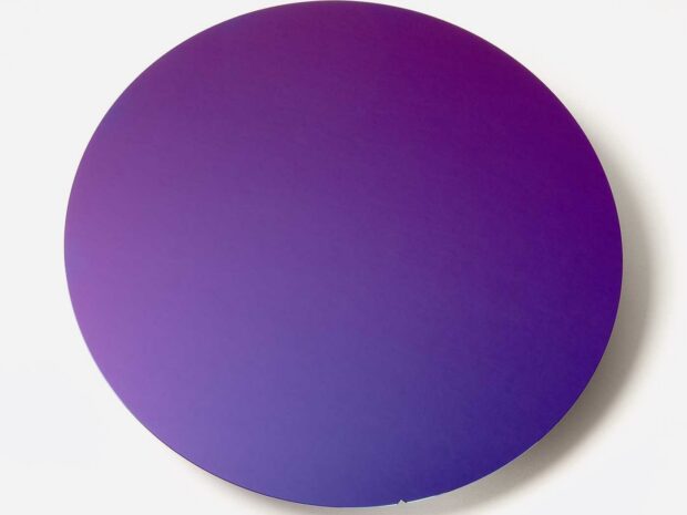
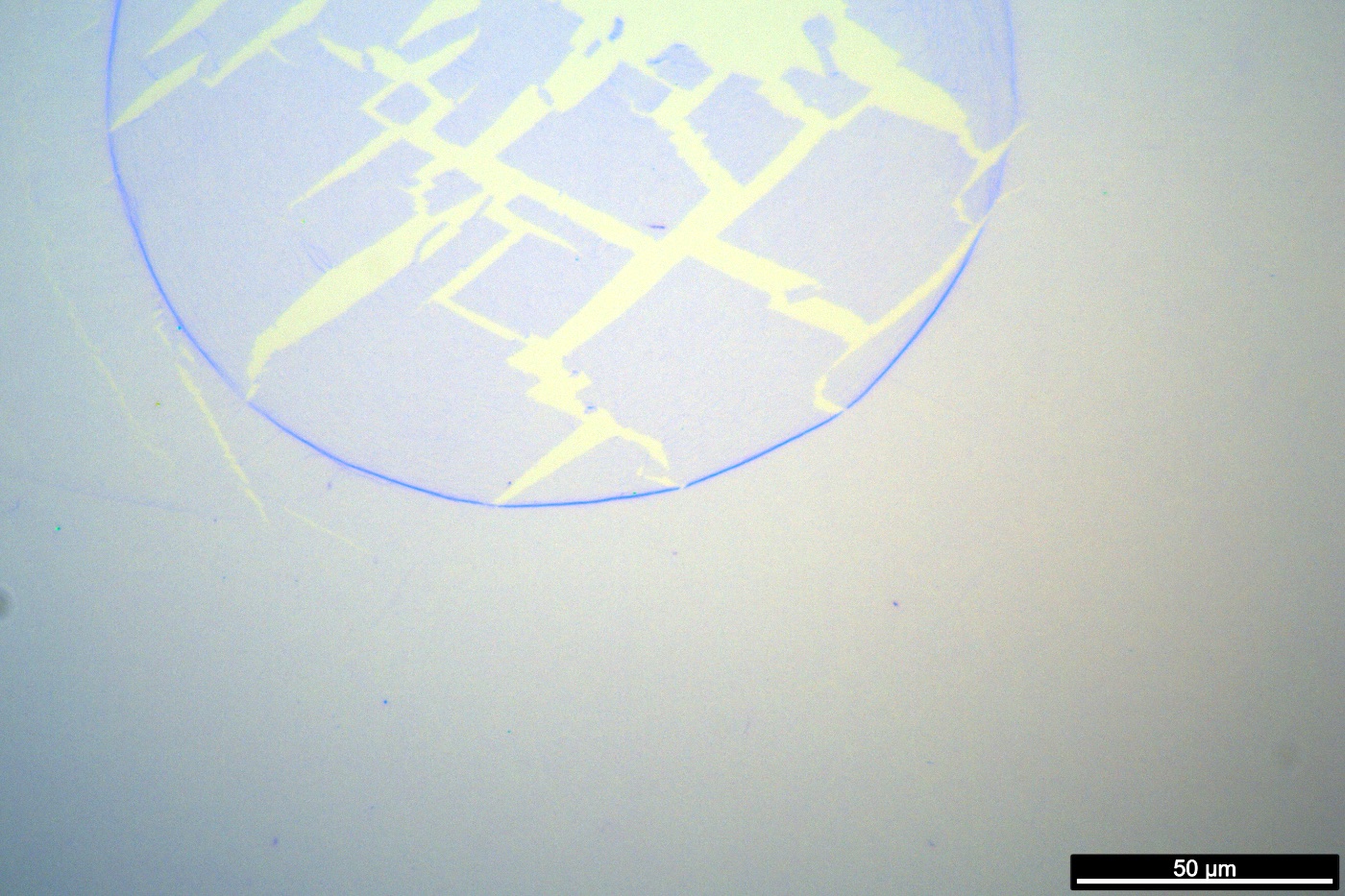
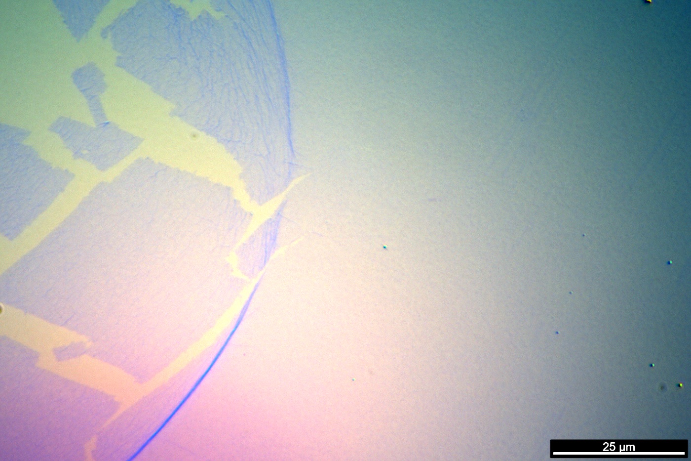
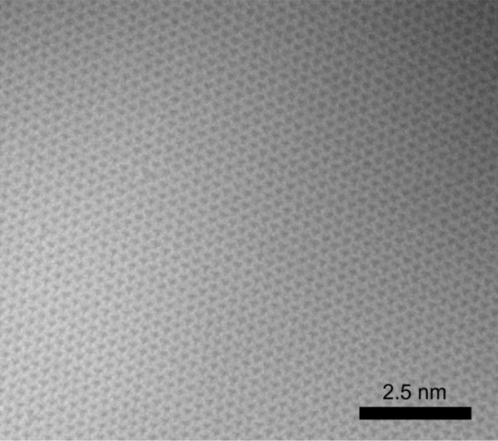
Single layer on transferred substrate
Monolayer hBN has a very small Raman cross-section, so Raman signals of this material are of very low intensity (compared to that of graphene, for example, or exfoliated multi-layer hBN)
Each sheet is vacuum sealed in a clean, inert nitrogen environment. Secondary packaging under positive nitrogen atmosphere, in a moisture-proof, light-proof, static-proof cleanroom bag, preserves the material between uses.
Store sealed, at room temperature, away from light. Open in a clean environment immediately before transfer.
Citing this material
Monolayer CVD hexagonal boron nitride on copper foil (HBN-CU-6), Grolltex, Inc., San Diego, CA. Cite the batch number printed on your specification sheet.
HBN-XFER
Monolayer hBN transferred onto your device substrate as a gate dielectric or encapsulation layer.
GRA-XFER
Monolayer graphene transferred onto Si/SiO₂, quartz, or the wafer you send us, up to 8 inches.
GRA-CU-6
CVD monolayer graphene film on copper foil. Single-atom-thick conductor for transfer onto your substrate, sensors, electrodes and heterostructures. In stock.
GRA-HBN
A layer of hBN beneath graphene. The close lattice match raises electron mobility for sensing and transistors.