GRA-XFER
Graphene transferred to your substrate
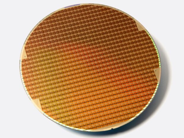
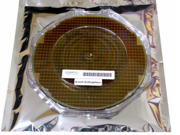
Monolayer graphene transferred onto Si/SiO₂, quartz, or the wafer you send us, up to 8 inches.
Request pricing
Details — Graphene transferred to your substrate

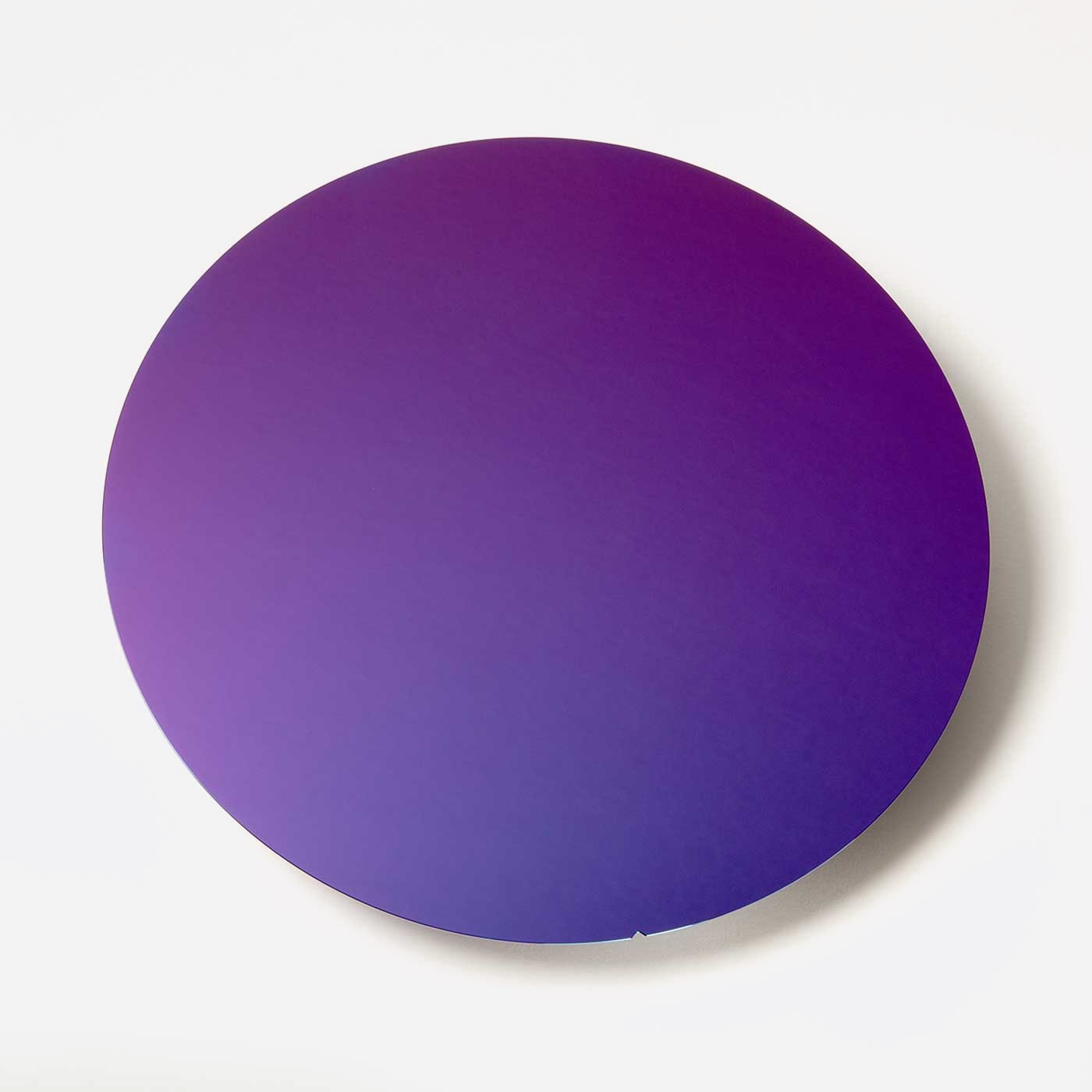
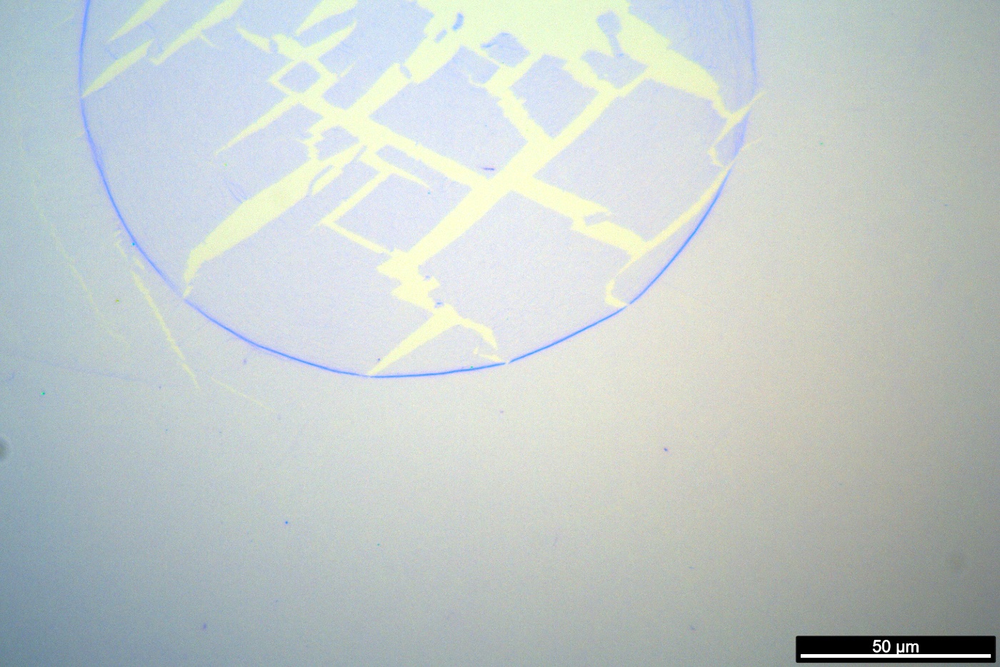
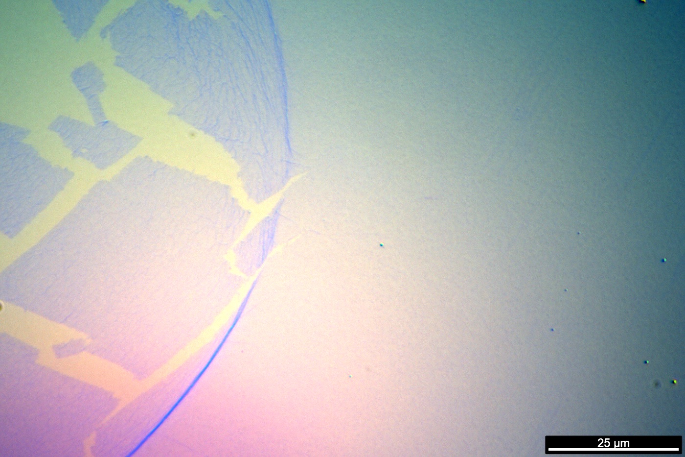
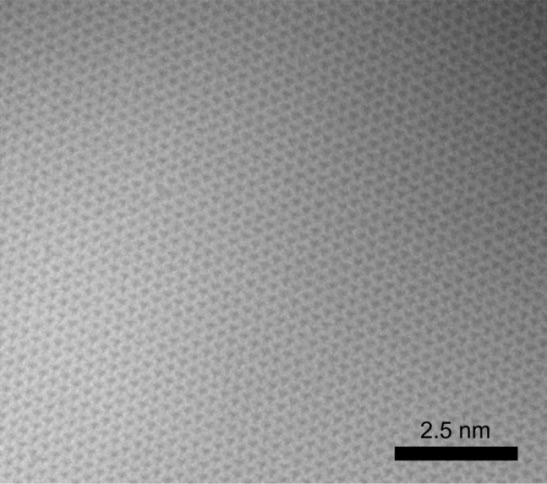
Monolayer hBN transferred onto your device substrate as a gate dielectric or encapsulation layer.
This configuration is quoted per order — sheet size, substrate and stack determine the price.
Request a quote| Specification | Value |
|---|---|
| Material | Monolayer hexagonal boron nitride |
| Max diameter | 8" (200 mm) |
| Standard substrates | Si/SiO₂, quartz |
| Custom substrates | On request |
| Band gap | ~5.9 eV |
| Fabrication | Class 100 cleanroom |
Representative data. The unit you receive ships with measurements from its own batch.

Exceeds refractory alumina (Al₂O₃)
Stacked by van der Waals interaction
Depends on substrate and volume
Citing this material
Monolayer CVD hexagonal boron nitride transferred to substrate (HBN-XFER), Grolltex, Inc., San Diego, CA.
GRA-XFER
Monolayer graphene transferred onto Si/SiO₂, quartz, or the wafer you send us, up to 8 inches.
GRA-HBN
A layer of hBN beneath graphene. The close lattice match raises electron mobility for sensing and transistors.
HBN-CU-6
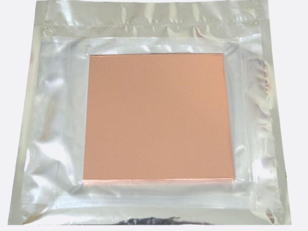
CVD monolayer hexagonal boron nitride (hBN) film on copper foil. Insulating 2D complement to graphene for dielectrics, encapsulation and heterostructures. Coming soon.
GRA-CU-6
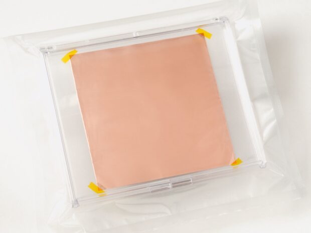
CVD monolayer graphene film on copper foil. Single-atom-thick conductor for transfer onto your substrate, sensors, electrodes and heterostructures. In stock.